Native CPUIF – openenoc_cpuif_if
Defines a native request and acknowledgement interface for register and scalar memory accesses.
Source: openenoc_cpuif_if.sv.
Parameters
Name |
Default value |
Allowed values |
Description |
|---|---|---|---|
|
|
Integer >= 1 |
Byte-address width in bits; connected interfaces must agree. |
|
|
Integer >= 1; AXI adapters require multiples of 8 |
Native data width and bit-enable width. |
Signals
Directions are relative to the named modport. The monitor modport, where present, observes signals as inputs and does not drive them.
Name |
Type |
Direction / role |
Description |
|---|---|---|---|
|
|
mst: output; slv: input |
Native access, lookup, or learning request. |
|
|
mst: output; slv: input |
Byte address presented to the native interface or decoder. |
|
|
mst: output; slv: input |
One selects a write; zero selects a read. |
|
|
mst: output; slv: input |
Native write data. |
|
|
mst: output; slv: input |
One enable per data bit for a native write. |
|
|
mst: input; slv: output |
Native write completion acknowledgement. |
|
|
mst: input; slv: output |
Native write error, valid with write acknowledgement. |
|
|
mst: input; slv: output |
Native read completion acknowledgement. |
|
|
mst: input; slv: output |
Native read error, valid with read acknowledgement. |
|
|
mst: input; slv: output |
Native read result, valid with read acknowledgement. |
Architecture and operation
Parameters and roles: ADDR_W and DATA_W default to 32.
Modports mst, slv, and mon describe the master, slave, and monitor.
Clock and reset belong to the connected modules rather than this interface.
The request/completion convention follows the PeakRDL-regblock native CPUIF.
req is a request strobe: the master presents the complete request with it
and waits for the matching read or write acknowledgement before issuing
another request. The slave captures any state needed after the request cycle;
the master need not hold req until acknowledgement.
addr is a byte address. req_is_wr selects write or read. wr_data
and wr_biten carry one enable per data bit, rather than per byte.
wr_ack and rd_ack complete their respective operations; rd_data
is valid with rd_ack. wr_err and rd_err are meaningful only with
their corresponding acknowledgement. The generated external RMEM boundary
exposes ACK/read data without ERR signals; see DMA Engine – openenoc_endpoint_dma_engine.
Functional scenarios
The examples use ADDR_W = DATA_W = 32. clk is the common clock of the
connected modules, shown only as a sampling reference; it is not an interface
signal. Each numbered cycle contains one rising sampling edge. Shaded x
regions mean a value is irrelevant to that operation, not that a driver must
drive an unknown value. Labels A0, A1 denote byte addresses, D0,
D1 denote data words, and M0, M1 denote per-bit write masks.
The labels are local to each diagram. The example latencies are illustrative.
Read request and returned data
In cycle 1, the master pulses req with req_is_wr = 0 and byte address
A0. The slave captures the request at that cycle’s rising edge.
The master deasserts req in cycle 2 and need not retain the address while
the read is pending. In cycle 4, rd_ack = 1 completes the read with
rd_data = D0 and rd_err = 0. The master samples the result at
the rising edge in cycle 4. wr_ack remains low throughout.
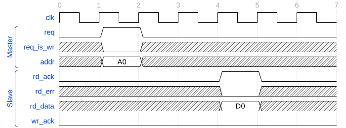
Read request followed by a delayed successful response
Write request with per-bit enables
In cycle 1, the master pulses req with req_is_wr = 1, byte address
A0, wr_data = D0, and wr_biten = M0. Each set bit in M0
enables the corresponding bit from D0. In an ordinary read/write
register, disabled bits retain their previous values:
new_value = (old_value & ~M0) | (D0 & M0)
For example, M0 = 0x0000000F enables only bits 3:0; the other 28 bits
retain their previous values. With old_value = 0xA5A5A5A5 and
D0 = 0x12345678, the masked update produces new_value = 0xA5A5A5A8.
Native masks can enable individual bits within a byte;
the CPUIF to AXI4-Lite – openenoc_cpuif_axil_adapter requires enables to be uniform within each
byte. Register-specific side effects can define different update semantics. The
request fields are needed only in cycle 1. The slave completes the write in
cycle 4 with wr_ack = 1 and wr_err = 0. rd_ack remains low, and
rd_data is irrelevant to a write.
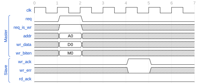
Native write with a per-bit enable mask
Immediate or delayed acknowledgement and target error
An immediate response presents the matching acknowledgement in the same cycle
as req. In cycle 1 below, the read request for address A0 completes
at the same rising edge with rd_ack = 1 and rd_err = 1. The read has
failed, so the master must not use rd_data as a successful result.
In cycle 3, the master issues a write to A1 with data D1 and bit mask
M1. The slave captures all request fields then, but asserts wr_ack
and wr_err only in cycle 6. The master keeps req low while waiting;
the error does not require the request strobe to remain asserted. These
symbolic address, data, and mask labels represent arbitrary stable values
during their request cycles.
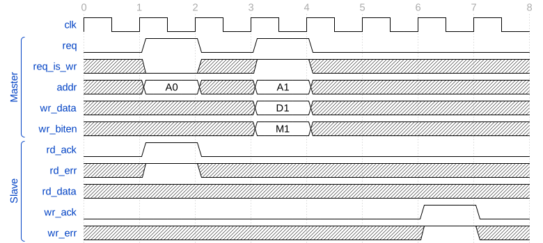
Immediate read error followed by a delayed write error
An error is qualified by its matching acknowledgement: rd_err without
rd_ack, or wr_err without wr_ack, does not complete an operation.
A failed access still completes and releases the interface for another
request. Successful immediate responses use the same timing with the
corresponding error signal low; delayed successful responses are shown in
the first two scenarios.